
Benefits of Single and Double-Sided Printed Circuit Boards
Benefits of Single and Double-Sided Printed Circuit Boards
The electronic industry uses Printed Circuit Boards for holding up electronic components securely. The board also helps in interconnecting the components such that the circuit can function most optimally. It is possible to obtain printed circuit boards in different types, such as:
- Single Sided
- Double Sided
- Multi-Layered
Fabricators can make very complex and sophisticated PCBs, depending on their application. For instance, all the above PCBs are also available as:
- Rigid PCBs
- High Definition Interconnect PCBs
The cost of a PCB board depends on its physical size, the number of layers making it up, and its manner of construction. A PCB offers several advantages that actually depend on its detail of construction.
Printed Circuit Board Construction
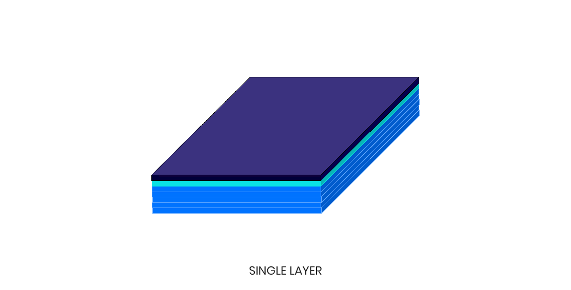
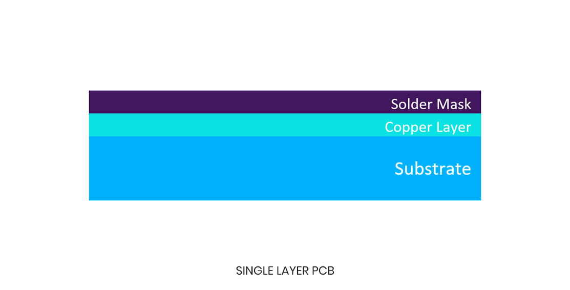
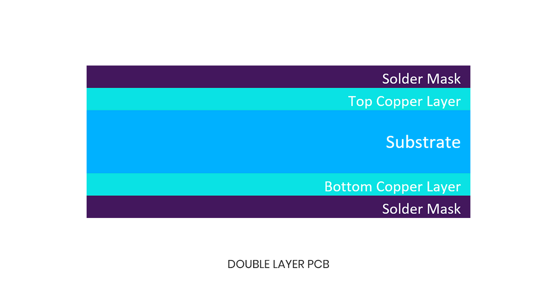
The printed circuit board gets its strength or rigidity from the core or substrate. The core is basically an epoxy reinforced glass fiber cloth. The fabricator bonds thin copper sheets on either side of the core, and this makes a copper clad. A single-sided board has only one copper sheet on the core, while the core of a double-sided board has both sides covered by copper.
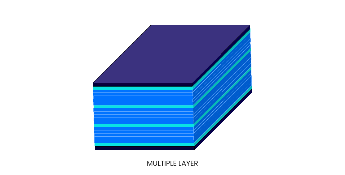
The construction of a multi-layered board is an extension of the double-sided board. It has several copper clads with a pre-preg or insulation bonding them together. PCB manufacturers can use different materials for making their boards rigid or flexible depending on the application. The type and construction gives the PCB its multiple advantages.
Benefits of Single-Sided PCB Boards
For the simplest and cheapest types of printed circuit boards, the industry uses the single-sided PCB boards. As there is only a single layer of copper, these boards can have only NPTH or non-plated through holes, and no vias. However, single-sided PCB boards are very well-suited for all types of components including through hole and surface mount components. Single-sided PCB board advantages include:
- Low costs, especially for high volume orders
- Simple construction
- Low probabilities of manufacturing issues
- Easy to manufacture
- Suitable for simple designs
- Suitable for low-density designs
- Faster lead times
Low Cost
Materials going into the construction of single-sided boards are readily available, which reduces their cost. Almost all PCB manufacturers make single-sided boards. The boards are inexpensive, as their fabrication does not require sophisticated tools or processes.
Simple Construction
With only a single core and one copper layer, the construction of a single-sided board is one of the simplest. A PCB fabricator must bond a copper sheet to a core and the single-sided board is ready.
Low Probabilities of Manufacturing Issues
With very simple processes necessary for the construction and manufacturing of single-sided boards, very little can go wrong. Therefore, there are very low probabilities of manufacturing issues cropping up. Most PCB manufacturers offer very high quality, low-cost single-sided boards.
Easy to Manufacture
During fabrication of a single-sided board, the manufacturer has to undertake only one complicated process—chemical etching, provided the board is for surface mount components only. An additional process such as drilling is necessary if the board is using through-hole components.
Suitable for Simple Designs
As the single-sided board has only a single layer of copper, the designer has very few channels between components for routing traces. Therefore, single-sided boards can accommodate only simple designs that have a low component count.
Suitable for Low Density Designs
In the absence of vias and plated-through holes, designers can implement only low density designs on single-layer boards. However, as they are the best suited for low-density designs, single-layer boards remain unparalleled for their cost and performance. In fact, single-layer boards are the first choice for most of the heavy copper designs for high-power circuits.
Faster Lead Times
With their simple and uncomplicated construction, single-layer boards are easy to fabricate. Combined with their low probability of issues, manufacturers can quote fast lead times for any single-sided board. In fact, it is possible to obtain single-sided boards from PCB manufacturers with a lead of one day.
Disadvantages of Single-Layer Boards
Although they have several advantages, there are several disadvantages of single-layer boards also:
- Unsuitable for medium or highly complex circuits
- Unsuitable for medium or highly density circuits
Designers overcome the above by using double-layer printed circuit boards.
Advantages of Double-Layer Printed Circuit Boards
A double-layer board can have vias and plated-through holes, which is its biggest advantage over a single-layer board. Using a via a designer can connect the copper layers on both sides of the core. Therefore, vias allow the designer to approximately double the number of channels available for routing traces. That increases the suitability of a double-layer board for use with circuits of medium density. Additional advantages of double-layer printed circuit boards are:
- Low costs
- Simple construction
- Low probabilities of manufacturing issues
- Ease of manufacturing
- Suitable for designs of medium complexity
- Suitable for medium-density designs
- Faster lead times
Low Costs
Although the presence of a second layer of copper makes a double-layer board more expensive compared to the cost of a single-layer board, the cost difference is marginal. The reason being the almost similar fabrication techniques for the two types of boards, with the addition of only an extra layer of copper.
Simple Construction
Even with the presence of two layers of copper, the method of construction still remains simple and similar to that of a single-layer board. Construction of multi-layered boards is even more complex.
Manufacturing Issues
The second layer of copper in the double-layer board does increase the probabilities of manufacturing issues. However, the issues remain far lower than those occurring in multi-layered boards.
Ease of Manufacturing
A PCB manufacturer must etch two layers of copper when manufacturing a double-layer board, while they etch only one layer of copper for a single-layer board. However, this does not increase the manufacturing complexity, as most manufacturers use the same bath for etching both sides at the same time. The drilling process remains the same for both types of boards for through holes and vias.
Design Complexity
In this area, the double-sided board has a clear superiority over the single-sided board. The presence of another layer of copper makes it possible for the designer to increase the number of traces while routing. Therefore, the double-layer board allows the designer to fit circuits of higher complexity.
Design Density
The presence of a second layer of copper and vias in a double-layer board serves to double the surface area available in a single-layer board of the same size. The designer now has greater freedom in breaking out traces from high-density components on a double-layer board.
Lead Times
With almost the same manufacturing process, for single-layer and double-layer boards, most PCB manufacturers offer similar lead times for both types of boards.
Low Costs
Compared to the cost of a single-layer board, the double-layer board is marginally more expensive. However, the increase in costs is far lower than those of multi-layered boards.
Conclusion
The industry uses single-sided boards for simple circuits, and double-sided boards for circuits with medium density and complexity, thereby optimizing costs in the long run. Space constraints in a design may force the designer to consider a multi-layered board. But if the designer can use a single- or a double-layer board, the project benefits from the lower complexity, lower costs, and low lead times.
