


PCB Design Guidelines for Fabrication

Improve the Design and Quality of your PCBs
PCB designers tend to concentrate their attention on electronic parameters. While keeping an eye on the large variety of components available in the market, selecting the most appropriate ones, and updating their component library is important for the design, they should also pay attention to the production capabilities of their PCB Manufacturer.
We highly recommend following some basic guidelines given below before you finalize your data package.
Want to understand the factors that impact the cost of PCB Fabrication?
Download our PCB Fabrication Cost Drivers resource to get insights into the factors influencing pricing and make informed decisions for your next project.
- Data Package
- Drill Layer
- Copper Layers
- Solder Mask and Legend
- Mechanical Layer
- Carbon Layers
- Peel-off Mask
- Via Fill
- Readme.doc File:
- Countersunk
Data Package
Should contain a PCB layout file with:
- All copper layers
- Solder mask and legend layers
- Board outline or mechanical layer
- SMD paste layers
- Carbon layers
- Peel-off layer, etc.
- All the above in a Gerber RS274-X format, and
- Drill file in Excellon-1 or 2 format with embedded tools list.
If possible, avoid sending data in Gerber RS274-D format as it is an obsolete format. If sending data in Gerber RS274-D format, make sure of including the aperture file along with the apertures used in the design.
It is not necessary to send PCB Design data such as:
- Original CAD data, Graphicode GWK files, PDF files, Word files (doc), Excel files (xls), parts lists, placement and assembly information, etc.
Wherever possible, check the generated output data (Gerbers & Excellon) with a Gerber viewer before sending to the supplier for PCB production. Make sure of including all instructions and/or other necessary inputs needed for fabricating the boards in the Gerber and Excellon files.
Use clear and easy to understand file naming and try to avoid long file names. Make sure it is easy to determine the layer function from the filename or else add a readme file for file identification. Avoid file names that are too long.
Do not provide scaled data. All data must be in full-scale, that is 1:1 ratio.
Make sure that Gerber files do not contain any apertures with zero-size (0.00 mm, 0 mils) and that Excellon data does not have any zero-sized tools (0.00 mm, 0 mils).
Use the same offset for all Gerber layers and Excellon drill data. Preferably use zero offset.
Use the same units (mm or inch) in Gerber & Excellon output files as in the CAD PCB design software. This will eliminate conversion or rounding errors.
Use the same resolution (grid) for Gerber & Excellon data to allow for a perfect match.
Make sure that data supplied begins from the top of the PCB and follows through to its bottom. Never mirror (or transform) any data layer, whether image or drill. Viewing a PCB from top to bottom through the board is the universal practice in the PCB industry. This means that when viewing Gerber data, text on the top side of the board (copper, solder mask, legend) should be readable and text on the bottom side (copper, solder mask, legend) should be non-readable (= mirrored).
Drill Layer
Make sure drill holes do not overlap, as this can cause broken drill bits and the small pieces of material left behind may cause voids in the barrels plated hole barrels.
Never use overlapping drill holes to define slots.
Manufacturers drill PCBs in steps of 0.05 mm (2 mils). Therefore, wherever possible, combine all drill sizes that are within 0.05 mm (2 mils) of each other.
If possible, provide separate drill files for plated (PTH) and non-plated (NPTH) holes. If this is not possible, always specify different tools for PTH and NPTH holes and mark them clearly.
If possible, never allow overlapping of NPTH holes on the board contour / outline, always consider it as a part of the outline and draw the correct outline.
For any PTH holes present on the board edge, mention it clearly in the mechanical layer.
Copper Layers
When generating output, preferably use “flashes” for pads and avoid “drawn pads” (i.e. pads filled with small draws)

Fig 1. Example of Drawn Pads
Never use drawn planes, i.e. filling large copper areas or copper planes with small draws (“painting”). Where possible, use contours or polygons to construct areas or planes. Using contours and filling areas with Polygon Area fill is a standard feature in Extended Gerber output (RS-274X).

Fig 2. Example of Drawn Pads
Include the board outline in copper layers. This will ensure a proper alignment of all layers in case there is an offset. At the same time, include the board outline in a separate Gerber mechanical plan.
Remove copper pads from NPTH holes if these pads remain unused or unconnected to other copper parts.
Keep copper pattern away from the board edge according to PCB manufacturer’s recommendations.
If it is necessary for the copper area or plane to extend up to the board edge, mention this prominently in the mechanical layer.
If it is necessary to plate the entire board edge or a part of it, mention this in the mechanical layer.
Use top viewed right-reading text to label every Gerber layer to prevent mirror board production.

Fig 3. Example of Top-Viewed Right-Reading Text Labeling.
Avoid peelables & same net spacing errors.

Fig. 4. Example of Peelable and Same Net Spacing Errors
Use full copper rather than hatch patterns in copper planes.
Always provide the proper layer sequence for a multilayer board. It is possible to indicate layer sequence in several ways: Indicate the layer numbers in the copper image by placing a logical number in each layer (1 for top layer, 2 for inner1, 3 for inner2, etc.).

Fig. 5. Example of Logical Number for Each Layer
If the plane layer design has strips of copper (sliver) between isolated pads, a minimum spacing of 0.20 mm (8 mils) is necessary between the isolated pads to avoid causing shorts due to resist lifting and re-depositing.

Fig. 6. Example of Sliver
Avoid thermal isolation.

Fig. 7. Example of Thermal Isolation
Adequately define all thermal relief pads to comply with the production requirement for Annular Rings (AR), Track Widths (Thermal Segment Width) and Gaps. Good practice for Thermals is to work with a Gap of 0.25 mm (10 mils) and a Thermal Segment Width of 0.20 mm (8 mils).
To avoid bow and twist problem, boards must have a balanced construction. It is a good practice to add redundant layers to make the board construction symmetrical around the central layer.

Fig. 8. Example of Unbalanced and Balanced Board Construction
Number and weight of copper layers should be symmetrical around the center of the stack up.

Fig. 9. Example of Unsymmetrical and Symmetrical Copper Layers
Place plane layers in stack up construction at symmetrical locations to minimize the risk of warpage.
Avoid low pressure area. Due to low pressure area, entrapped air in the laminated panel does not allow flow of air and resin and it causes micro-voids in laminated multilayer boards or may cause delaminating problem. Add venting or copper pattern in the inner layers to equalize pressure distribution.

Fig. 10. Example of Solder Mask
Do not place pads or traces too close to the PCB edge.
Pads or traces placed too close to the PCB edge may get damaged during routing or scoring—leading to copper exposure, oxidation, or structural failure.
To prevent this, we recommend maintaining a safe clearance between copper features and the board edge during layout.
Click here to check minimum recommended values.
Following these guidelines ensures smooth manufacturability and long-term reliability of your PCBs.
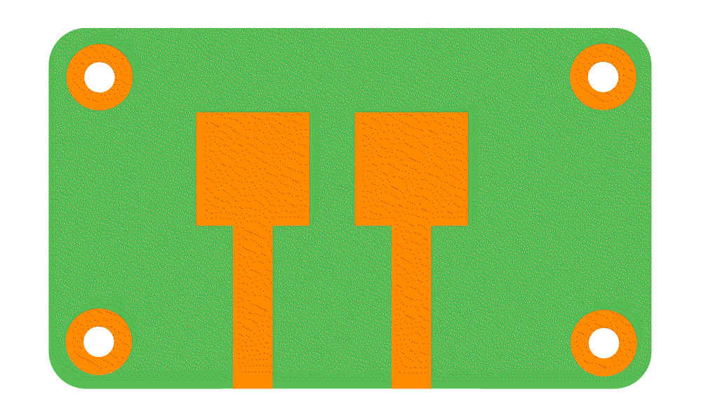
Fig. 11. Example of copper pads too close to PCB edge
If the inner layer annular ring is too small, there is a risk of breakout—causing open connections, reduced reliability, or structural failure of vias.
To prevent this, ensure the annular ring meets or exceeds the minimum supported values for inner layers in your design.
Click here to check minimum recommended values…
On outer layers, insufficient annular ring reduces solderable land area and increases the chance of breakout during drilling. This can result in poor solder joints, open circuits, or weakened via reliability.
Maintain the required annular ring clearance for outer layers to avoid such issues.
Click here to check minimum recommended values...

Fig. 12. Inner/Outer Layer Annular Ring (IAR/OAR) error
If the outer layer isolation is below the supported value, risks include short circuits, solder bridging, or etching defects during fabrication.
Follow the minimum isolation requirements to ensure electrical integrity and manufacturing yield.
Click here to check minimum recommended values...
For inner layers, isolation and track width must be designed considering the final copper thickness. If isolation is too small or tracks are too narrow relative to the specified finish copper, issues such as over-etching, shorts, or impedance mismatch may occur.
Design with proper clearances and track widths to align with the supported copper thickness for reliable performance.
Click here to check minimum recommended values...

Fig. 13. Inner/Outer Layer Isolation error
Solder Mask
Typically, solder mask should have a minimum of 0.10 mm (4 mils) “growth/mask opening” around the pad to allow for any mis-registration.
The minimum solder mask “dam” should be 0.10 mm (4 mils) (a dam is the minimum track size of solder mask). Once the “dam” goes below 0.10 mm (4 mils), it becomes more difficult to process as the “dam” can lift from the PCB surface.
Non-green masks require wider mask openings and bigger mask dams than necessary for green masking.
Make sure solder mask openings are not too close to copper traces.
When solder mask openings are too close to nearby traces, those traces may be unintentionally exposed, leading to oxidation or shorts during soldering.
To avoid such risks, always maintain a minimum clearance of 0.10 mm between pads and adjacent traces in your solder mask design.
Following this recommendation improves soldering reliability and ensures better assembly quality.
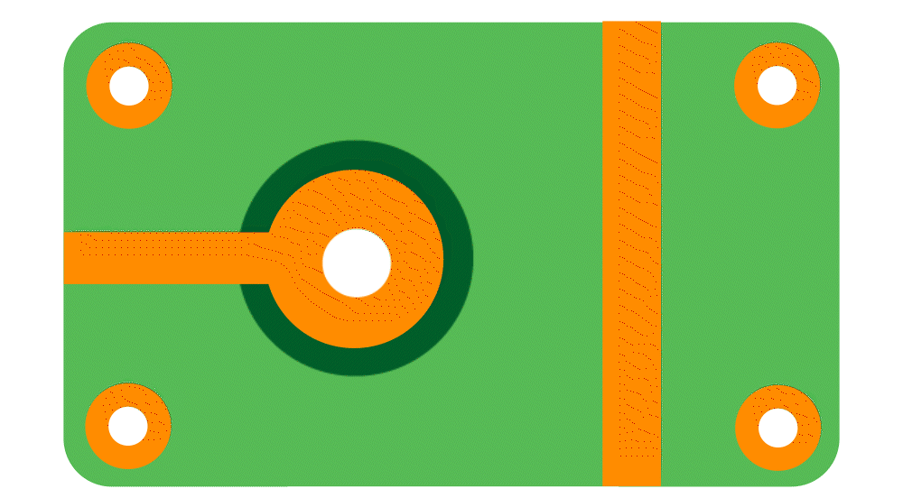
Fig. 14. Example of solder mask too close to copper traces
Legend
For Legend printing, the main consideration is font size / height. Fonts with height less than 1 mm (40 mils) may become non-readable after printing.
Break or clip any legend print that tends to overlap solder mask layer to make sure the legend ink does not cover the pad. This helps improve soldering.
Keep line width for font at 0.10 mm (4 mils). Remove any line thinner than 0.10 mm (4 mils).
Minimum text height for legend should be 1.00 mm to ensure readability after fabrication.

Fig. 15. Example of Legend Print
To avoid clipped legends, maintain a minimum distance of 0.20 mm (8 mils) between legend elements and the copper image.

Fig. 16. Example of Legend Clipping
For PCB fabrication, maintain minimum legend clearances from:
- PCB edge: 0.25 mm (routing), 0.45 mm (scoring)
- Exposed copper: 0.10 mm
- Holes and cutouts: 0.10 mm
For PCB assembly, ensure adequate spacing between legend and components to avoid interference during placement, especially for fine-pitch designs.
Mechanical Layer
A mechanical layer should contain at least:
The exact board outlines, ideally including dimensions (in mm or inch).
Exact positions and sizes for all internal milling, slots or cutouts, ideally including dimensions (in mm or inch).
While providing dimensions, always take the center of the contour lines as the actual outline of the board, regardless of their thickness.
Additional information to include in the mechanical plan as necessary:
A reference hole: X and Y distances of the drill hole center from the PCB outline. This is particularly important when there are NPTH holes without copper pads.
Positional indication of all drills using symbols (in drill map). Use different symbols for each of the different drill sizes.
PTH/NPTH indication for holes and slots
A clear layer sequence or buildup drawing including all copper layers, solder mask and legend layers, any additional layers such as peel-off or carbon, in the correct sequence viewed from top to bottom and with the correct corresponding data file name.
If the PCBs are to be delivered as an array for assembly, include the mechanical drawing for the array as well.
GKO vs Mechanical Layer — What's the Difference?
While the mechanical layer provides detailed board outlines and fabrication instructions, GKO (Keep-Out Layer) specifically defines areas where no components, traces, or copper should be placed — typically for design rule enforcement, not for manufacturing reference.
For a detailed explanation, refer to our blog on GKO vs Mechanical Layer.
Carbon Layers
Mention unambiguously the side of the PCB for applying carbon. This can be on one side or on both sides. Indicate the position by naming the file properly and describe a clear buildup or layer sequence in the mechanical layer.
When generating the output include the board outline in the carbon layer(s).

Fig. 17. Example of Carbon Layer on PCB
Overall carbon design rule specifications:
- Minimum carbon line width: 0.30 mm (12 mils)
- Minimum carbon to carbon spacing: 0.254 mm (10 mils)
- Carbon pad should be 0.15 mm (6 mils) bigger than copper pad.
- Mask pad should be 0.15 mm (6 mils) bigger than copper pads.
- Mask pad is same size as Carbon pad.
Peel-off Mask
Generally, peel-off mask is applied only to one side of the PCB, usually the bottom side.
If Peel-off is necessary on the top side of the PCB or on both sides, please mention this properly by means of suitable file naming and describing the clear buildup or layer sequence in the mechanical layer.
When generating the output include the board outline in the carbon layer(s).
Avoid using many small peel-off areas randomly placed on the PCB. Wherever practical, make the peel-off area as large as possible by connecting separate peel-off areas. This will make it easier to remove the peel-off after soldering.
Overall peel-off design rule specifications:
- Minimum width of any Peel-off element (P): 0.500 mm (20 mils)
- Maximum coverable hole ENDSIZE (H): 6.00 mm (0.236 inches)
- Minimum overlap on copper pattern (V): 0.254 mm (10 mils)
- Minimum clearance to free copper (W): 0.254 mm (10 mils)
- Minimum distance from PCB outline: 0.500 mm (20 mils)
- Tolerance on position: +/-0.300 mm (12 mils)

Fig. 18. Example of Peel-Off Mask
Via Fill
Completely closed via holes can only be guaranteed by using Via Fill.
The maximum via hole end size that can be completely closed is 0.25 mm (10 mils).
Via Fill means covering the via pad and via hole with a second layer of solder mask.

Fig. 19. Example of Via Fill
Provide Via Fill data as a Gerber file containing only the via pads that need filling and include the board outline.
Do not forget to include the board outline in your Via Fill layer.
Typically, Via Fill is applied only on one side of the PCB, with the board design defining the side.
Mention unambiguously the side of the PCB (top or bottom) to apply the Via Fill. Use proper file naming and clearly describe the buildup or layer sequence in the mechanical layer.
Readme.doc File:
Avoid annoying questions by attaching a readme file with the following details:
List of file names and descriptions
Details of the Gerber format in case of Gerber-d files
Details of PTH / NPTH holes
Details of any other special requirements
Also add answers to frequently asked questions such as:
Remove non-functional pads in inner layers?
Add copper thieving for better plating?
Any logo placement restrictions?
Add "teardrop" at trace and pad intersections?

Fig. 20. Example of Tear-Drop at Intersection of Trace and Pad
Is it acceptable to place a void rim if a non-plated through-hole passes through a copper land?

Fig. 21. Example of Void Rim
If spacing is inadequate for placing solder mask dam for a fine pitch SMT package, is gang opening acceptable?

Fig. 22. Example of Gang Opening
If hole size tolerances are missing, is it acceptable to use +/- 0.075 mm (3 mils)?
If PCB thickness tolerances are missing, is it acceptable to use +/- 10%?
If PCB size tolerance missing, is it acceptable to use +/- 0.25 mm (10 mils)?
Countersunk
Countersunk is basically creating a conical-shaped indentation on the surface of a hole, typically for the purpose of allowing a screw or bolt to sit flush with the surface of the PCB.This process is commonly used in electronic assembly to ensure that there are no obstructions or protrusions that may interfere with the mounting of other components or devices on the PCB.The countersunk hole is created by drilling a larger diameter hole at the top of the hole, and then gradually tapering the diameter down towards the bottom of the hole.This creates a conical-shaped hole that can accommodate the head of a screw or bolt, allowing it to sit flush with the surface of the PCB.
If you require a countersunk drill in your mechanical drawing, please provide the necessary information for mapping the drill diameter with a note specifying the countersunk requirement.Please include an image in the mechanical drawing showing the actual values you need. Our team will ensure that your requirements are met for a precise and accurate design.


