


PCB Assembly Design Guidelines (DFM)
Design Guidelines PCB-A
PCBs are a critical component of all significant electronic devices. Hence, when you are assembling one or working with our team to get one assembled, it is essential to be on the same page when defining the best practices, terminology, and modus operandi.
Despite the continuous development in the space, there are several essential terms & practices which are yet to be standardized. For such terms & practices, our team has made an attempt to provide the necessary explanations before we delve into any further details.
The PCB Power team has perfected these guidelines over years of practice, observation, and feedback. We believe it will help you minimize errors, lead-time, and processing costs in the PCB Assembly lifecycle.
- Input Data Requirements
- Component Types
- Package Types
- Foot Print Review
- Paste Layers Review
- Bill of Materials Review
- Component Placement Review
- PCB Layout and Design Review
- Panel Edge to Component Clearance Best Practices:
Data Requirements
The assembly process is dependent on two key datasets:
- Bill of Materials (BOM) or Parts List:This list comprises every part used in assembling and manufacturing the PCB. It generally includes a file that enlists the parts along with their description, Manufacturer’s Part Number (MPN), Supplier’s Part Number (SPN), and Reference Designators (R1, C2, IC3, etc.). The list must be as comprehensive as possible and include the components that are to be used for assembling the parts for the PCB.
- Component Placement List (CPL):As the name suggests, this file directs the PCB Assembly process by dictating the precise position, degree of rotation, and the designated side of the board, along with the reference designator that has to be populated. The file is frequently called the Pick & Place File, Centroid File, XY File, and Position File.
Component Types
-
Through-Hole Technology: The technology encompasses a process of mounting leads into holes drilled through the PCB. The other side of the component is soldered to ensure
stability.
Plated Through Holes are a common variant of the technology. Under this process, the capillary suction effect applies to the holes filled with solder. The result is a relatively stronger bond.
As soldering is done on the opposite side of the component, lead times and error rates can be dramatically reduced by having all the components mounted on one side of the PCB.
Some of the most common soldering techniques include using a solder wave machine, a selective solder wave machine, a manual soldering process, or a pin-in-paste soldering process. In the latter approach, solder paste is applied through the PCB across the component holes. Once the components are accurately placed, the PCB is processed in a solder wave oven. - Surface Mount Technology: With this process, a reflow oven is used for soldering the component leads, which are placed on copper pads that sit on the surface of a PCB. The copper pads ensure a mark for all the component leads on the PCB to maintain accuracy.
- Mixed Technology: This process integrates both the Through Hole Technology and Surface Mount Technology for SMD connections on the PCB. This method brings the best of both technologies and is ideal for power devices and connectors.
Package Types
| Category | Dimensions |
|---|---|
| Smallest Package for Passive Components | 01005, 0201, 0402 |
| BGA |
1. 0.65 mm Pitch for QFN 2. Maximum 0.4 mm Pitch for QFP |
| Maximum Component Package Size for Soldering | 56 x 56 x 15 mm |
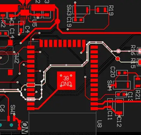
Foot Print Review
Here are the best practices to ensure an efficient process:
- Ensure that your components and pads are perfectly aligned across all the layers. Use the datasheet to provide accurate markings and identifications.
- If the design does not have room for the recommended drill size in a through-hole process, ensure that the drill is 0.15 mm larger than the lead’s size.
- Fine pitch SMT components should have minimum solder masking between the pads. Our team recommends 0.08 mm solder masking with 0.06 mm for green mask color, 0.12 for other colors, and 0.10 mm for mask opening. The masking should be minimum but sufficient to avoid short circuits between pins.
- If the surface mount pad sizes are not in the right shape or are imbalanced because of trace sizes, it can result in an effect called ‘tombstoning’ – one pad would reflow faster than the other one and asymmetrically lift one end of the pad.
Paste Layers Review
- The solder paste layer should be in a 1:1 ratio with the designated circuit layer’s pads.
- Make sure you have added fiducials in the paste layers.
Bill of Materials Review
- The BOM must include:
- MPN for each component and its quantity for 1 PCB/Array.
- Each component should have a unique identity created with a reference designator and description that matches the information available in the BOM.
- Use readily available components to avoid longer lead times.
- With each update for the components, change the part numbers.
Component Placement Review
- Avoid placing the components near the board's edge. This can damage the board during the assembly & manufacturing process.
- Use SMT parts on one side of the board. Having them on both sides will increase the costs and complicate the process.
- If the components are placed too close, the pick & place machines might provide an erroneous output. Even the testing for such designs is challenging and resource-consuming.
- While using discrete components, ensure that the pins enter the solder simultaneously as the board passes through the wave. Having larger parts precede smaller parts can result in insufficient solder between pins and metal pads.
- Some parts will get hotter at a rate faster than the other ones. Hence, ensure that such parts are optimally placed for airflow and distance from other similar parts.
- Avoid using parts with idiosyncratic dimensions near smaller SMT parts. This makes the soldering process all the more challenging.
- Place connectors optimally, relative to other system-level boards and interfaces with sufficient room for plugging & unplugging cables in the assembly process.
PCB Layout and Design Review
While the exact dimensions and size of the PCB may vary to align with your design requirements, here are the ideal dimensions that can be easily accommodated:
| Category | Dimensions |
|---|---|
| Minimum Board Size | 90 mm x 50 mm (Smaller sizes will be panelized) |
| Maximum Board Size |
500 mm x 300 mm (Standard Components) 150 mm x 150 mm (for components pitch less than or equal to 0.5 mm BGA/QFP/QFN) |
| Board Thickness |
0.5 mm to 1.00 mm (Board size up to 150 mm x 150 mm can be accommodated) (For thinner boards, confirm the panel requirements with the assembly team.) |
| Maximum Board Thickness | 3.2 mm |
| The Shape of the PCB |
Rectangular, Circular, and Idiosyncratic Shapes (All shapes other than rectangular ones will require panelized boards in an array and panel borders on at least two longer sides.) |
Panel Edge to Component Clearance Best Practices:
- Components can be mounted on individual boards or the boards organized in panel form.
- The sides of the panels and boards must have at least 3 mm of space that keeps the active circuit components away from the edges.
- Arrays are necessary for overhanging components. Add additional clearance between PCBs if the designs overlap at the edge. This will reduce the assembly cost by enabling component mounting on the PCB while it is still in a panelized format.

