Fool-Proof Way to Minimize PCB Design & Manufacturing Gaps
Fool-Proof Way to Minimize PCB Design & Manufacturing Gaps
PCB design is not an easy process. The exact functioning of a critical device might depend on how you have designed the PCB. That is why it is perfectly natural for PCB designers to get sleepless nights when they have turned in the design files to the manufacturer. But, there has to be a better way to do this! We have devised a solution to make sure your PCB design fits your requirements. Let's explore it and a few other steps you can take in the pre-production stage to avoid reworks, delays, and sub-optimal PCB performance.
-
Understand Your Manufacturer’s Design Guidelines
Go to the PCB Power Market website and go through our design guidelines. Additionally, you can check our technical capabilities and set your Design Rule Check accordingly. This will give you a preliminary idea of whether your design meets our basic manufacturing standards or not.
-
Try Different Vantage Points
Usually, as a designer or an engineer, you might have spent countless weeks working on each element on the PCB. You might have zoomed in several times and looked through each minute detail. While this is a great exercise, it can make you distant from the larger picture – how all the elements come together on the printed circuit board. To take a step back and see the entire picture – you can use Gerber data in different environments, analyse your design from different angles, and get a second opinion on your design.
-
Physical Inspection
Once you have examined the design from different examples, take a physical print in a 1:1 ratio and study it thoroughly. This will highlight any disproportionate issues you might have in the design. You can even place sample components to see if the design is coming out the way you expected. Look for topics such as inter-connector clearances and other minute discrepancies.
-
Pre-Production Approval
Here is an industry secret – your submitted design data does not go into manufacturing precisely the way you share it with the manufacturer. Since it would be nearly impossible to change the manufacturing process for the design data, most manufacturers make small but immaterial changes in the design data to fit it within their manufacturing process. Such changes can include but are not limited to maintaining clearance between silkscreens, using copper to fill out gaps, etc., which make the PCB more reliable. We follow the same practice and inform you the moment we discover that the changes will result in a statistically significant difference in your design functionalities.
The Pre-Production Approval feature is a streamlined process to virtually examine every element of your design data and let you know if any material changes are required to manufacture your design. It includes thorough documentation on the tools used at this stage and provides you assurance on the quality & performance standards of your PCB.
The process puts a much-needed buffer between your order and the design going into the irrevocable manufacturing phase. With each day between the two, you and our team will have more time to review the design files and decide if any substantial design changes are required.
To better understand the process, you can have a look at these two screens:
- Image 1:
This shows the number of files shared with you during the process. While the screen shows only one file open at the moment, you will have full access to a comprehensive range of files to examine how our process can meet your design constraints specifically.

- Image 2:
.png)
This set of documents contains a zip file with every single file necessary for your explicit approval. You can explore the layer identification fil to understand every exception as made available in the list given here with the help of a digital number and an identification number:
- 01: Tope Circuit Layer
- 02 to 15: Inner Circuit Layer
- 16: Bottom Circuit Layer
- 21: Topmask
- 31: Botmask
- 22: Topsilk
- 32: Botsilk
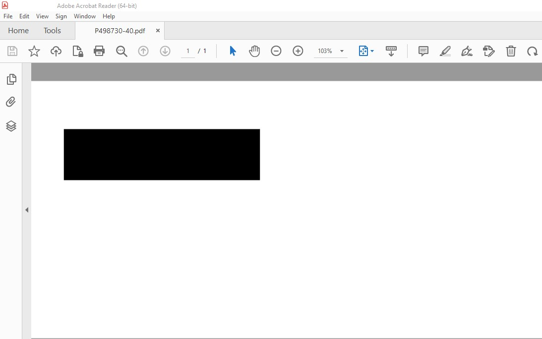
- 40: Outline
- 60: Drill
- 61: Routing
- 62: Score/V-Cut
- 63: Drillmap
The PXXXXXX-01 and PXXXXXX-16 represent the respective top and bottom layers. The numbers between PXXXXXX-02 to PXXXXXX-15 represent the inner layer 2, layer 3, layer 4, and the subsequent layers in that order. The PXXXXXX-21 illustrates the top mask layer, and the PXXXXXX-31 represents the bottom mask layer. Finally, the PXXXXXX-22 and PXXXXXX-32 represent the silk layers.
The outline layer is represented in a contour of the required shape & size, and the black area represents the circuit board's outer board once the cutting process is done.
- Image 1:
How to Access the Pre-Production Approval Feature?
-
Click on the Pre-Production Approval option while placing your order.
-
Or, write an email to us with all the order details included at [email protected]. Our team will reach out to you the moment your design has been processed so you may review the production data. And, if you had registered your email address during the order placement, you can get an instant review/update post designing process.
.png)
To know more about how PCB Power Market can help you transform your PCB designs into functional products, get in touch with one of our experts by clicking here.


