How to avoid delays for your order?
Incomplete Data Package
One or more data files necessary for production are missing. For example: for a double sided job, one of the circuit layers is missing or the order detail shows that silk is required on both sides but the data package contains only one silk layer. We can’t start the production with the missing files. We have to raise an exception for the missing inputs and put the job on hold till we get the complete data package. Minimum required files in the data package are:
- Files for all physical circuit layers
- One or two mask layers as per their requirement
- One or two silk layers if they are required
- Excellon drill files with tool details (PTH, NPTH, Blind/ Buried drills)
- Outline layer
- Readme file / Mechanical drawing stating file identification / buildup detail and for technical requirements of your order.
- Apertures file in case of Gerber-D format.
Unaccepted Data Format
We accept PCB layout data in the following formats:
- Gerber RS274-X (Extended Gerber with embedded aperture data)
- DPF (Dynamic Process Format – developed by Mania Technologies NV)
- Gerber RS274-D (Standard Gerber with separate aperture file(s))
We prefer a Gerber file in a RS-274X format. This will eliminate the need for the PCB manufacturer to load apertures during the tooling process. We accept drill and profile data in the following formats:
- Excellon + appropriate tool-list (we accept Excellon 1 and Excellon 2)
- Sieb & Meyer + appropriate tool-list (we accept Sieb & Meyer1000 and Sieb & Meyer3000)
We prefer ASCII-encoded drill files. Drill and profile data can also be supplied in Gerber (RS-274X or RS274-D) or DPF.
No Design Files
We do not accept design files because, we would need legal copies of the design software used for the respective designs. This seems impossible; as designers do not always use the same CAD package with the same software version. On the other hand, a Gerber file is unambiguous, which has been the standard format for PCB fabricators for many years. For Eagle users, we will use Eagle *.brd to Gerber274x.
Missing Layer Sequence
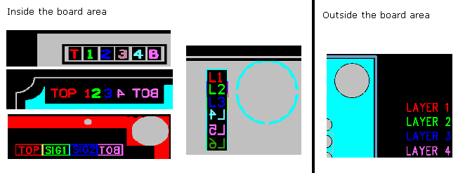
All CAD systems do not use the same naming convention; similarly, all designers don’t use the same default layer sequences. As a manufacturer, we will raise an exception, because only the designer can give you the correct layer sequence for his/her PCB. You can indicate the layer sequence by adding the layer number in the copper layer with a traditional number line sequence in each layer (1 for top layer, 2 for inner1, 3 for inner2, etc.). Make sure the numbers are positioned in such a way that they do not overlap, and can be seen through the complete PCB.

Or add stackup detail in the mechanical layer in the correct sequence and with the correct corresponding data file name.
| LAYER STACK-UP | DESCRIPTION | |
|---|---|---|
| No | Name | |
| 1 | TOP (LAYER 1) | Base Cu Foil 18micron (Finished copper should be atleast 0.035mm) |
| 0.35mm Prepregs | ||
| 2 | GND (LAYER 2) | 0.035mm Copper |
| 0.71mm Laminated Core | ||
| 3 | VCC (LAYER 3) | 0.035mm Copper |
| 0.35mm Prepregs | ||
| 4 | BOTTOM (LAYER 4) | Base Cu Foil 18micron (Finished copper should be atleast 0.035mm) |
Layer readability is not clear
.png)
Correct layer naming makes sense only when the readability of the layer is correct. Layer readability is to identify the right reading of the layer from the respective side of the board. In simple words, to identify the given layer is top layer/bottom layer viewed from top side or from bottom side. In the absence of any text in the circuit layer, it is difficult to guess the correct readability of the layer. In such a situation, we have to put the job on hold and wait for the confirmation from your end. Use a top view right-reading text to label every Gerber layer to prevent mirror board production. Or put a text outside the board outline with a correct readable format and also, with the layer identification. Or add a pdf file with image of each layer stating the respective layer identification and readability.
Missing Outline Layer
Providing outline layer is the most common method that is used for communicating how to cut the ordered PCBs. A board outline layer needs to be included with your data package. Gerber files are preferred, but we can make an outline from a dimensioned drawing with sufficient information of how to align it correctly relative to the circuitry. Providing the actual routing layer instead of outline layer: Routing data generation is production specific requirement which, may differ from one fabricator to other. Each PCB fabricator has their own rules for giving a routing order, compensation and direction for milling the PCBs. Hence, we need to make it at our end and we can’t use your sent routing layers. Also, there are possibilities that we misinterpret your requirement for compensation if it is clearly not mentioned that the given routing layer is already compensated or not. Do not provide actual routing layer only outline layer is enough for us to know the shape and cutting of your PCBs. Silk files are generated using less than 1 mm character height: For legend printing, the main consideration is text height and line width. Generally, legend files are generated using 8 mil to 10 mil line width. In most cases, this is acceptable if the height is proportional. For small dimension parts / letter height, 8 mil to 10 mil line will blur during the application process.
Specifications for Legend Print:
- Minimum Legend Line Width: 0.15mm (6mil)
- Minimum Text height for good readability: 1.00mm (39.5mil).
.jpg)
Design rules beyond our capabilities
Check the design rules before uploading the order; make sure the design should not be beyond our capabilities. This results in the cancellation of the order. Please refer our design rules as shown below: General Board Specifications
- Laminate: FR-4
- PCB Thickness: 0.8mm / 1.6 mm/2.4mm
- Start Copper Thickness: 17.5 Microns/ 35 Microns/ 70 microns
- Min. Track Width/ Spacing: 0.17/ 0.15mm (7 Mils/ 6 Mils)
- Min. Hole: 0.40mm (16 Mils) Finish
- Min. SMD Pitch: 0.5mm (20 Mils)
- Solder mask: Green/ Blue/ Black
- Surface Finish: Hot Air Leveling (HAL)/ Lead Free HAL/ Immersion Silver/ Immersion Gold (ENIG)
- Legend: White/Black/Yellow (White is default , other colors are subject to availability, please contact our sales team for further details.)
Product Specifications
- Please refer the link: http://www.pcbpower.com/technology/technical-capabilities/ for our capabilities.
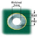
Please keep in mind for Annular ring calculation, we follow the below given formula Annular Ring = 1/2 (Circuit layer pad diameter – PHD) Where PHD = Production Hole diameter or Tool ize = finihed hole size + 0.15 mm for Plated through holes = finished hole size + 0.05 mm for Non Plated through holes
Minimum Annular ring for Outer layers: 0.125 mm Minimum Annular ring for Inner layers: 0.125 mm IMPORTANT:Annular Ring calculations are done from the production TOOLSIZE for the holes, not from the finished hole ENDSIZE. For connected non-plated (NPTH) holes we recommend a minimum annular ring of 0.50 mm. As NPTH holes have no plated barrel, a smaller annular ring may be lifted during soldering or break away even during normal operating conditions.


