Let’s go through a brief description of all the steps involved in the process of PCB designing Part -1
For an efficient circuit board design, it’s important to understand the design process and that is what our blog is all about. It provides you a brief description of all the steps involved in the process of our printed circuit board designing and also guidelines that help to create an error-free design, fulfilling the fabrication requirements.
Since there are quite a lot of steps involved, we have divided the process into two fundamental parts:
Before the Design:
Before the Design:
Initially it is just the beginning of the concept or the idea of the design that takes shape. Before the design, all you would require is to select a list of components to be used, data sheet of each component and the components to be used in the electrical schematic.
Then you create a schematic diagram of the board and decide where and how the board fits – whether it fits in a case or cabinet or simply slides into a rack with guide rails or mounting holes?
Define the electrical hierarchy- Define the inputs, outputs or displays as well as the sources of obtaining power or exchanging information.
Determine the mechanical/electrical requirements – Is there any height restriction? Where should the critical components be located?
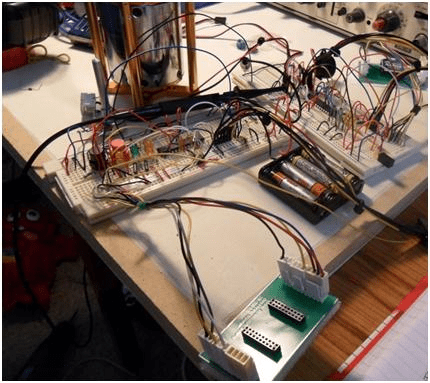
It would be preferable if you have the components hand soldered onto breadboard in the earlier stage of the design so that the conflicts if any may be cleared then and there. It would also serve to conduct several different implementations of the feature, benchmark the resulting performance and ensure the correct design decisions.
We hope this blog will be very useful to indurstend PCB design process .We will come back with part -2 next week .