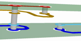
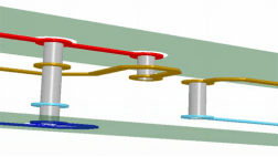
The Why and How of Switching Layers – from 1 or 2-layer to 4-layer and higher
The ever persistent miniaturization of electronic products triggers the manufacture of more densely packed printed circuit boards with increased electronic capabilities. Unfortunately, the lack of enough available space makes it challenging for the single sided and double sided PCBs to match the increasing assembly density.The Significance of available space for routing the traces in switching from 1 or 2-layer to multilayer
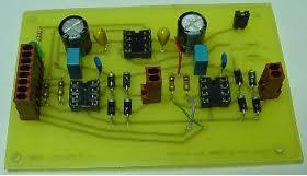
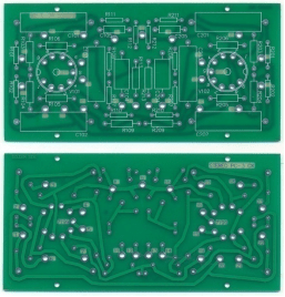
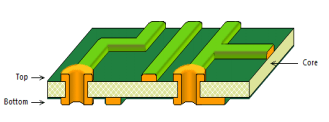
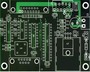
It is a well-known fact that the most basic Single Sided boards have their components mounted on one of their sides and the conductor pattern on the opposite. Such boards have severe limitations when it comes to routing the traces in the conductor pattern. Since it is only on one side that no traces can cross, and have to be routed around each other, it is used merely in very primitive circuits.




.png)
