
What Are Vias And Why Do You Need Them?
Just as a printed circuit board (PCB) is a means to allow interconnection of different components, vias are means to interconnect different layers on and within the multilayered PCBs. Also, just like there are various types of PCBs, there are multiple types of vias with their own functionality. Simply put, vias are Plated-Through Holes (PTHs) passing through one or more layers in a PCB, connecting traces on its way. IPC defines seven types of vias in IPC-50M, Terms and Definitions for Interconnecting and Packaging Electronic Circuits. These are:
Type I: Tented Vias—vias that have a mask material applied, bridging over them, with no additional material inside the holes.
Type II: Tented and Covered Vias—type I vias with a secondary covering of mask material over and above the tented vias.
Type III: Plugged Vias—vias with material partly penetrating into the via holes.
Type IV: Plugged and Covered Vias—type III vias with a secondary material covering the vias.
Type V: Filled Vias—vias with material fully penetrating and encapsulating the via holes.
Type VI: Filled and Covered—type V vias with a secondary material covering the vias.
Type VII: Filled and Capped—type V vias with a secondary metalized coating covering the vias.
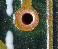
Fig. 1: Close-up of a Via
Although small and sometimes very small, vias are extremely important parts of the circuit board landscape. In fact, in the world of surface mount components, vias are the only means to interconnect copper traces on different layers on a PCB, where earlier, leads of components would do the job when soldered on both sides of a two-layer PCB. The only difference between plated-through holes and vias is no component lead will ever pass through the hole of a via.
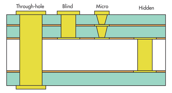
Fig. 2: Different Types of Vias
Each of the seven types of vias classified above may be further subdivided into three types depending on their functionality—blind or hidden vias, buried vias, and through hole vias. As the name suggests, through hole vias travel through the board, connecting traces on the outermost layers, and if required, on the inner layers as well. Blind vias start on the surface on one side of the board, but do not extend to the other side, finishing on one of the internal layers instead. Buried vias remain completely encapsulated within the board, and none of their ends extend to any of the outer surfaces of the board.
Most vias in high-density boards have very small-diameter holes, and are called micro-vias. Manufacturers use different tools such as ultrasonic beams and lasers to drill these holes. Usually, micro-vias are filled with a conductive material to facilitate connecting with the pad on the other layer. However, this can lead to issues with unequal expansion as explained later.
Tented Vias
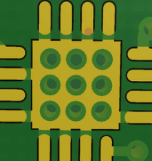
Fig. 3: Tented Vias
The word “tenting” in the PCB industry originally meant the solder mask would enclose the via fully in the form of a skin or tent over the hole. This was difficult for manufacturers to achieve with liquid photo-imageable (LPI) solder mask, as the success of the process was dependent on the diameter of the hole and surface tension of the LPI. With the introduction of dry film solder mask, manufacturers achieved tenting easily, but the process was more expensive.
With LPI, tenting caused the mask to cover the pad and enter the hole partly. However, this was not consistent, as some vias remained unplugged, and others had the tent broken over the hole, covering only the annular ring or pad. Therefore, as per requirement, manufacturers resorted to plugging vias with conductive or non-conductive materials before tenting with LPI.
Tenting is useful for reducing the number of exposed conductive pads present on the PCB, and helps in reducing the likelihood of shorts from solder bridging during the assembly process. In the case of SMT pads, tenting helps to reduce paste migration away from the pads of SMD components when vias are placed either on the ends of their pads or on the dog-bones meant for BGAs.
Additionally, tenting is helpful whenever vias are placed close to SMT pads, especially in areas within the BGA package, where shorts can easily happen under the component during reflow, making rework difficult and time-consuming. Covering the tented via with a secondary coating of solder mask often helps,
Disadvantages of Incomplete Tenting
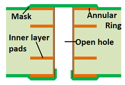
Fig. 4: Incomplete Tenting
Although tenting of vias by primary LPI solder mask is advantageous as it is only a single step process, the process cannot guarantee complete tenting, resulting in long-term reliability issues. Successful tenting by screen coating depends on the size of the hole, surface tension of the liquid mask, and the board thickness. As no surface finish is applied to the via barrel before tenting, incomplete tenting may cause entrapments. Usually, this is chemical entrapment from preclean lines when enhancing surface finish.
Preclean lines subject surface finishes to a micro-etching process, allowing micro-etchants to be trapped in the open vias, where the chemical crystallizes rapidly to generate copper-sulfate crystals. Over time, these crystals etch away the copper in the barrel, causing long-term reliability issues. For instance, the gold of the ENIG finish could form a galvanic cell with the exposed copper near the top of the via in the presence of the micro-etchant chemical, thereby accelerating the process of etching.
Incomplete tenting may also cause solder paste to wick into the via, leaving insufficient paste to complete the actual soldering. In the case of BGAs, localized thermal energy may cause the LPI solder mask to lift between the ball and the via capture pads, as the distance between them is very short, causing solder shorts.
Above issues with incomplete tenting has led to manufacturers plugging vias with solder mask or some other non-conductive or even conductive materials. The plugged via does not require surface finish to be applied to the via barrel, but does ensure that subsequent application of the LPI mask leaves all the vias fully tented.
Vias Plugged with Non-Conductive Fill
For vias plugged with solder mask or similar non-conductive epoxy material, the manufacturer has to ensure the via is completely plugged and sealed, and its annular ring is fully covered. This is a common practice when using BGA SMD pads to prevent solder wicking into the via creating poor or non-existent solder joints.
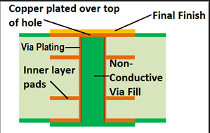
Fig. 5: Active Pad
However, with BGA packages becoming tighter, it is becoming increasingly difficult placing vias on standard ‘dog-bone’ land patterns for transferring signals to other layers. This difficulty has led to vias being drilled directly into the pads of the BGA footprint. The process is known as via-in-pad, and allows much simpler routing. Although this requires the via hole to be fully plugged, it also requires the surface of the plugged via to be plated over with copper, and subsequently flattened and planarized to be even with the surrounding copper features. Therefore, with the application of the final finish, there is a solderable surface mount pad, also called an active pad, capable of passing signals to inner layers, eliminating the need to place vias on the surface layer for the purpose.
Vias Plugged with Conductive Fill
Some chips generate a lot of heat, which must be conducted away to prevent the chip from overheating. Placing thermal vias plugged with conductive fill under the chip helps in the process, as the metallic nature of the fill naturally wicks the heat away from the chip to the other side of the board, just as a radiator does. This technique is helpful even in cases where a chip draws high currents, as multiple vias plugged with conductive fill reduce the resistance of the track, thereby lowering the voltage drop between the voltage source and the pins of the chip.
Drawbacks of Conductive Fills
Vias filled with conductive fill generally present a different coefficient of thermal expansion (CTE) between the surrounding laminate and the metallic fill. With heat, metals expand much more rapidly than the surrounding laminate does, leading to a possible fracture between the pads and the hole wall. Therefore, where the purpose of the fill is only to reinforce the copper pad plated over the hole, designers using via-in-pad do not recommend the conductive filling process.
Conclusion
Designers often try to match the CTE of the conductive fill for vias with that of the surrounding material. This is important in the view of the board living out its life in a heating/cooling state, where the expansion and contraction of the materials can lead to stress fractures in vias and possible electrical opens in the worst cases. However, this consideration generally favors the non-conductive epoxies for via filling as their CTE matches that of the laminate more closely, making the PCB a more reliable product.
