Why is a Printed Circuit Board Necessary and How to Design it?

Those involved with electrical and electronic equipment are also familiar with the term Printed Circuit Board or PCB. However, not many know about the origins of printed circuit boards, their uses, and requirements for designing them. Although highly sophisticated at present, printed circuit boards were not always this way. In fact, before PCBs came into existence, people would interconnect components with wires. Even with simple circuits, this exercise was fraught with errors, and susceptible to frequent failures. Insulation on wires would crack due to age, and short circuits were frequent.
Then someone discovered the stability of wire-wrapping. By wrapping a thin wire around a metal post, it was possible to set up a highly durable connection at individual points. Moreover, the advantage of wire-wrapping was a gas-tight connection, but easily changeable. However, the joys of wire-wrapping did not last long, as electronics was moving on to integrated circuits, and to Surface Mount Devices or SMDs. At the same time, original equipment manufacturers or OEMs were substantially increasing the complexity of their products and the number of electronic components in each product. Consumers were demanding smaller equipment with better features. The development of modern printed circuit boards came as a relief to OEMs and a boon to consumers.
Functions of Printed Circuit Boards
Copper traces present on a printed circuit board serve to replace point-to-point wire connections, with the base or substrate acting as a non-conducting supporting board. The top surface of the board has the provision to mount necessary electronic components, anchoring them in place with solder. The assembled and soldered PCB therefore, becomes a major sub assembly within an electronic device. Apart from fixing the electronic components to the board mechanically, solder binds the component leads to the copper pads on the PCB providing a good electrical connection.
Types of Printed Circuit Boards
The industry uses several types of printed circuit boards with different complexities. As a broad classification, there are:
- Single-Layer Boards
- Double-Layer Boards
- Multi-Layer Boards
Single-layer boards have copper traces on one side of the substrate. These can support circuits of low complexity. For higher complexity in smaller sizes, there are double-layer boards with copper traces on both sides of the substrate. For highly complex circuits, even double-layer boards may not be enough, and designers must use multi-layer boards. Multi-layer boards have several layers of copper separated by insulating prepreg material and vias interconnecting the traces on each layer. Modern computer boards with 16+ layers are an example of multi-layer boards.
Parts of Printed Circuit Boards
A PCB gets its rigidity from its central non-conducting core or substrate, usually made of paper phenolic or glass epoxy. There are special non-rigid or flexible PCBs also, with a central core material of Kapton or Polyimide. Around the central core a double-layer board has two thin layers of copper. The combination of copper layers bonded to a central core has the commercial name of copper clad. A single-layer board has only one copper layer. For a multi-layer board, a fabricator will bond additional copper layers on the copper clad with insulating prepreg material in between.
The outer layers of a printed circuit board often have a protective green insulating mask or solder mask. This mask covers almost 90% of the board, leaving out the pads meant for soldering components. Flexible printed circuit boards use Coverlays rather than solder masks.
On the solder mask or coverlay, designers use a silkscreen layer. This layer adds letters, numbers, and symbols on the PCB surface in contrasting colors, aiding assembly. A silkscreen label may indicate the polarity of an LED, a diode, the orientation of ICs, or the function of connector pins.
Advantages of Using Printed Circuit Boards
The major advantage of using a printed circuit board is the orderly organizational mounting it offers to all electronic components making up the equipment. Not only that, it also provides a standardized insulation between all the components, thereby allowing them to function properly without shorting or heating up inadvertently. Along with the tiny SMDs, PCBs allow the designer the freedom to create smaller and more compact electronic equipment.
Designing Printed Circuit Boards
Designing a printed circuit board requires some understanding of its fabrication process. The copper clad is the substrate with a copper layer on one or both its sides, depending on whether the board will be single-sided or double-sided. The designer makes up the pattern of traces that will remain on the copper layers according to the PCB circuit design. The fabricator uses a lithographic process to transfer the pattern onto the copper layer, and chemically etches away the unwanted copper. The fabricator them drills the necessary holes for vias and to accommodate through-hole components. He/she then uses an electroplating process to add a thin layer of copper over the traces, and forming the side walls of the holes at the same time. After this, the fabricator uses a solder mask covering to protect the copper traces, and adds a silkscreen layer on top.
Size of Printed Circuit Boards
Since a PCB must hold all the components on its surface, physically placing them together forms the basic estimate of the size of the board. Accommodating the PCB assembly within the equipment may require further adjustment to the physical size of the board. If it is not possible to accommodate the PCB assembly, the designer has the option to use smaller components for the PCB circuit design, or to increase the equipment size. Usually, the outcome is a compromise between the two options. Once the designer has finalized the physical dimensions of the PCB and its method of mounting, they can start with the layout and placement of the components according to the PCB circuit design.
Layout and Component Placement
Rather than physical components, designers use their footprints. A footprint is an accurate drawing of the amount of physical space a component will occupy on the surface of the board. They place all the footprints within the boundary of the printed circuit board, and arrange them for the shortest interconnectivity. For example, a printed circuit board that will connect to a panel using a connector, should have the connector on an edge of the board nearest to the panel. Similarly, the designer will place all components associated with an IC as close to it as possible so that the interconnection length is the shortest.
Manual PCB Circuit Design
In the early days of manual PCB circuit design, designers used a base Mylar sheet and created the footprints and interconnections out of self-adhesive tapes and pads, arranging them in four times the regular size. After completion of the design, an industrial camera recorded the design on photographic film reduced to the actual size. The fabricator used this film to transfer the pattern of traces onto the copper layers. This method is no longer in use, as powerful computers and PCB circuit design software packages have replaced it.
Computer Aided PCB Circuit Design
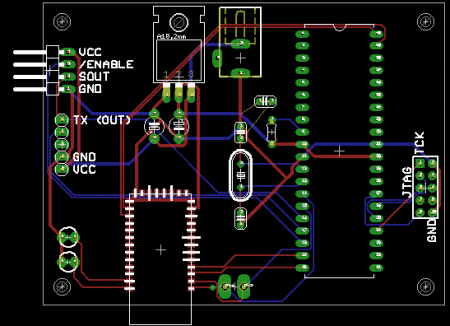
Today designers use CAD of computer aided design for handling all types of PCB circuit design. There are mechanical CAD systems for designing the equipment and the outer dimensions of the printed circuit board. For the PCB circuit design, there are PCB CAD software packages that help with schematic design, footprint creation, library creation, PCB layout, and routing of traces.
A CAD PCB circuit design package usually has a database of the symbols, footprints, and other details of common electronic components that designers frequently use. These software packages usually work in three parts. The first part is for schematic capture or drawing the circuit schematic. The second is the auto router part for laying out the footprints and interconnecting them effectively. The third part is for generating the necessary output files for the fabrication process.
For drawing the circuit schematic, the designer selects symbols of various components from the database of the software package. The database also has many footprints associated with each symbol, and the designer must carefully select the specific footprint they will use. While drawing the PCB circuit design, the software keeps a track of the interconnections the designer has made between different components, and generates a net list.
Depending on the footprints selected by the designer, the auto router places them within the boundary of the PCB. Following the net list, the auto router then creates a maze of interconnections. Some software packages have the capability to rearrange the footprints in the most optimal manner, while allowing the designer to override this capability.
After completing the rearrangement, the auto router proceeds to interconnect components with traces, creating vias as necessary. To prevent traces from overlapping, the auto router may use traces on other layers, connecting them with vias. Usually, the traces are of default width, but the designer can change the final width of specific traces, allowing the auto router to reroute and accommodate the changes.
Sometimes, the auto router may fail to complete the routing within the specified number of layers. The designer must add more layers to complete the routing. In the PCB industry, Gerber files are the standard for transferring manufacturing information from the designer to the fabricator for manufacturing printed circuit boards.


